Table Of Content
Summit Interconnect’s eight facilities feature cutting-edge capabilities, ultra-efficient processes, the most experienced teams, and a culture dedicated to exceeding expectations. Summit has extensive experience supporting the semiconductor industry across many applications including ATE boards, probe cards, reference boards, and substrates. In the medical sector, we excel in miniaturization and power-efficient designs for wearable medical technology, adhering to ISO standards. See the top reasons why every electronics designer needs MCAD software.
EAGLE's Layers
Parts can be placed on many sheets and connected together through ports. If you have a specification or a list of requirements for your device, then we can pre-select the components you need and prepare a preliminary bill of materials (BOM). We can also make arrangements with manufacturers and vendors of customized components for your device.
Processor Architectures
The gold lines, called airwires, connect between pins and reflect the net connections you made on the schematic. There should also be a faint, light-gray outline of a board dimension to the right of all of the parts. PCB composition is all about layering one material over another. The thickest, middle part of the board is a insulating substrate (usually FR4).
Step 3: Adding the Power Input
They Used To Be A Big Shot, Now Eagle Is No More - Hackaday
They Used To Be A Big Shot, Now Eagle Is No More.
Posted: Fri, 09 Jun 2023 07:00:00 GMT [source]
If you see a black gap separating a pad and the pour, there is no connection. If you see some traces forming a "target" over the pad, there is a connection from the pour to that pad. You can (and probably should) have ground pours on both sides of the board, so follow the same set of steps on the bottom layer. Next, draw a set of lines just like you did the dimension box. In fact, just draw right on top of the dimension lines.
Start drawing at the origin, trace all the way around, and finish back at the same spot. A dotted red box should appear around the dimension of the board. Vias are really tiny drill holes that are filled with copper. We use them mid-route to move a trace from one side of the board to the other. Our job will be turning each of those gold airwires into top or bottom copper traces.
Eagle Software Download. Autodesk EAGLE is a PCB (Printed… by plchmiservo - Medium
Eagle Software Download. Autodesk EAGLE is a PCB (Printed… by plchmiservo.
Posted: Sat, 03 Feb 2024 08:00:00 GMT [source]
Paste can only be used to paste a group that has previously been copied to your clipboard. To use paste you first have to create a group, then (with the copy tool selected) CTRL+right-click to copy it, but hit ESC instead of gluing it down. This'll store the copied group into your operating system's clipboard, and you can use paste to place it somewhere. This tool is especially useful if you need to copy parts of one schematic file into another. After selecting the part you want to add, it'll "glow" and start hovering around following your mouse cursor.
Autodesk Fusion ECAD Tutorial
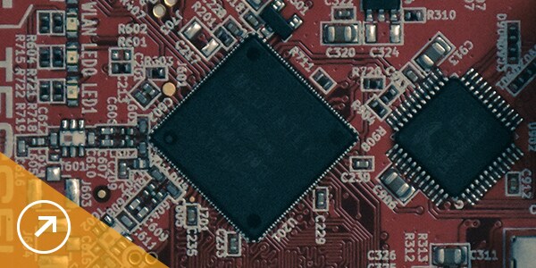
Yellow circles (on this design, but they're more often green) called "vias" pass a signal from one side to the other. Bigger vias allow for through-hole parts to be inserted and soldered to the board. Other, currently hidden, layers expose copper so components can be soldered to it. Project folders are like any regular file system folder, except they contain a file named "eagle.epf". The EPF file links your schematic and board design together, and also stores any settings you may have set especially for the project. We'll start by making a new project folder for our design.
Checking the Board
You could add labels for the headers, or values for the resistors, or even create a nifty logo. Before we package the design up and send it off to the fabrication house, there are a few tools we can use to check our design for errors. There are tons of optimizations and settings to be made in the autorouter. If you want to dig deeper into the subject, consider checking out EAGLE's manual where an entire chapter is devoted to it. Make sure you leave enough space between two different signal traces. If you need more precise control over your routes, you can hold down the ALT key on your keyboard to access the alternate grid.
What is Autodesk Fusion?
After processing the routing variants you evaluate the results and choose the best one for you. You can get anywhere from one to 12 layers on your board. Such PCBs can accommodate more components than a standard double-sided board. They are lightweight, small-sized, and more powerful.
We are not just a PCB design company; we are your trusted partner in bringing your electronic devices to life. Stay connected with the latest news, knowledge and tutorials for EAGLE and electronics design. Create the next generation of products with a unified schematic, PCB, library management, simulation and mechanical design on a single design platform. The customer receives a fully functional device or software and a detailed user manual. After finishing the project, we provide a free warranty period, during which the team will eliminate any discovered defects and bugs.
With more than 20 years of dedicated experience in PCB layout services, we bring precision, efficiency, and innovation to each project. Learn all about the capabilities and benefits of using one platform for all your product design needs. As part of our BSP development services, we create low-level operating system code, device driver code, and other files with... Integra Sources has long-lasting and successful relationships with trusted enclosure designers. We will provide consultation and help you place an order.
It allows back-annotation to the schematic and auto-routing to automatically connect traces based on the connections defined in the schematic. With over 45 years of expertise in printed circuit board (PCB) fabrication and design, Bay Area Circuits is uniquely qualified to handle your PCB design and layout projects. It is available in the toolbar (left side of the window). You can interact with these icons by drag and drop with mouse.


No comments:
Post a Comment